USD
 INR

Call Us Now
+91 9106756572
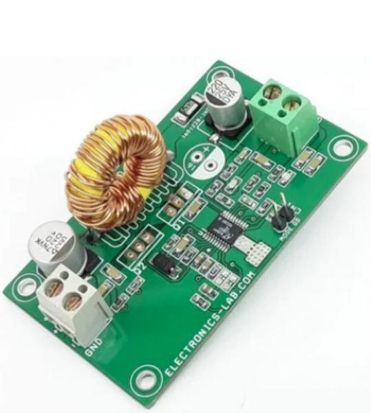
The project presented here is a low quiescent current, synchronous buck converter featuring the LTC3807. This DC-DC converts a 16V to 38V input voltage to a 12V at 6A output. The main features of this board include an internal LDO for gate drive power from VIN or EXTVCC, RUN pins, a mode selector jumper CN1 that allows the converter to run in constant current mode (CCM), pulse-skipping or Burst Mode operation, and selectable current limit. Output is fixed and provides 12V DC but it supports an adjustable output voltage. Refer to the datasheet below to learn more about the adjustable output. The circuit has also soft-start and tracking. The wide input voltage range of 16V to 38V is suitable for automotive and distributed DC power systems where the low quiescent current is essential. The operating frequency is set to 120Khz using resistor R6. MOSFETs are mounted under the PCB for easy heatsink mounting, it is important to use a heatsink for a full current load.
The project presented here is a low quiescent current, synchronous buck converter featuring the LTC3807. This DC-DC converts a 16V to 38V input voltage to a 12V at 6A output. The main features of this board include an internal LDO for gate drive power from VIN or EXTVCC, RUN pins, a mode selector jumper CN1 that allows the converter to run in constant current mode (CCM), pulse-skipping or Burst Mode operation, and selectable current limit. Output is fixed and provides 12V DC but it supports an adjustable output voltage. Refer to the datasheet below to learn more about the adjustable output. The circuit has also soft-start and tracking. The wide input voltage range of 16V to 38V is suitable for automotive and distributed DC power systems where the low quiescent current is essential. The operating frequency is set to 120Khz using resistor R6. MOSFETs are mounted under the PCB for easy heatsink mounting, it is important to use a heatsink for a full current load.
The LTC3807 uses a constant frequency, current mode step-down architecture. During normal operation, the external top MOSFET is turned on when the clock for that channel sets the RS latch and is turned off when the main current comparator, ICMP, resets the RS latch. The peak inductor current at which ICMP trips and resets the latch is controlled by the voltage on the ITH pin, which is the output of the error amplifier, EA. The error amplifier compares the output voltage feedback signal at the VFB pin (which is generated with an external resistor divider connected across the output voltage, VOUT, to ground) to the internal 0.800V reference voltage. When the load current increases, it causes a slight decrease in VFB relative to the reference, which causes the EA to increase the ITH voltage until the average inductor current matches the new load current. After the top MOSFET is turned off each cycle, the bottom MOSFET is turned on until either the inductor current starts to reverse, as indicated by the current comparator IR, or the beginning of the next clock cycle.
Mini Isolated Power Supply is designed for CAN, RS-485, RS-422, RS-232, SPI, I2C, Low-Power LAN applications. The power supply provides +/- 5.50 V DC symmetrical outputs with load current 500mA from 5V DC input. The project is built using SN6505A IC from Texas instruments. The SN6505A is a low-noise, low-EMI push-pull transformer driver, specifically designed for small form factor, isolated power supplies. It drives low profile, center-tapped transformers 5 V DC power supply. Ultra-low noise and EMI are achieved by slew rate control of the output switch voltage and through Spread Spectrum Clocking (SSC). The SN6505 consists of an oscillator followed by a gate drive circuit that provides the complementary output signals to drive ground referenced N-channel power switches. The device includes two 1-A Power-MOSFET switches to ensure start-up under heavy loads. The internal protection features include a 1.7A current limiting, under-voltage lockout, thermal shutdown, and break-before-make circuitry. SN6505 includes a soft-start feature that prevents high inrush current during power up with large load capacitors.
This is a versatile tiny module that provides 10V/500mA from 90V DC input. It is a high voltage input DC-DC buck converter, based on LM5017 IC, which is a 100-V, 600-mA synchronous step-down regulator with integrated high side and low side MOSFETs. The constant on-time (COT) control scheme employed in the LM5017 requires no loop compensation, provides an excellent transient response, and enables very high step-down ratios. The ON-time varies inversely with the input voltage resulting in nearly constant frequency over the input voltage range. A high voltage startup regulator provides bias power for the internal operation of the IC and for integrated gate drivers. A peak current limit circuit protects against overload conditions. The under-voltage lockout (UVLO) circuit allows the input under-voltage threshold and hysteresis to be independently programmed. Other protection features include thermal shutdown and bias supply under-voltage lockout (VCC UVLO). Supply input range 13V to 90V, provides 10V/500mA, switching frequency 225 KHz. Adjustable output voltage possible by altering Resistor R6 and R8 value, refer data sheet. Under-Voltage lockout set to 12.4V.
The project presented here is capable of supplying 400mA of current from a 3.7V Li-Ion/Li-Po Battery input with a 5V output. The converter has an internal soft start and internal frequency compensation features. The project is built using LTC3426 SOT23-6 chip. The LTC3426 chip is in a low profile (1mm) SOT-23 package and has a very low shutdown current of about 0.5µA. A switching frequency of 1.2MHz allows a tiny solution. The tiny PCB can be mounted on the backside of the a 18650 battery holder. Jumper J1 is the shut-down jumper. Internal soft-start eases inrush current issues.
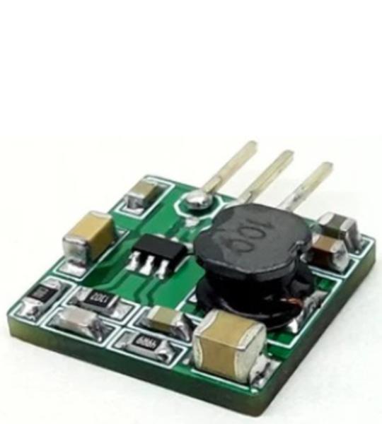
This tiny power module is an easy-to-use integrated power solution that combines a 3A DC/DC converter chip with inbuilt power MOSFETs, an inductor, and passives into a 3-pin, through-hole package. The standard TO-220 pin-out allows a much-improved replacement of linear regulators packaged in this industry-standard footprint. The circuit provides much higher efficiency and output current without the need for a heatsink. This is an easy replacement of the LM7805 linear regulator with higher input voltage and output current than LM7805. Operating supply 8-28V DC, output 5V DC at 1A. The project is built using the TPS54302 chip from Texas instruments.
This is a multiple output power converter module that provides +/-10V (Dual 10V), 5V DC, and 3.3V DC from a 9V PP3 battery. This is a very useful project that has been designed for low-load current applications. Dual +/-10V output from a 9V battery is a key feature of the project. The battery holder can be mounted on the backside of the PCB. An onboard slide switch provides power ON/OFF. Onboard LED indicates the power. LM1117-5V chip provides 5V DC output from 9V Battery, further, an LM1117-3.3V regulator is provided to step down the 5V to 3.3V DC. MAX680 charge pump chip provides +/-10V from 5V.
Cookie preferences