USD
 INR

Call Us Now
+91 9106756572
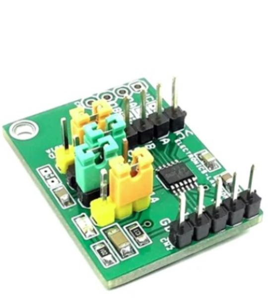
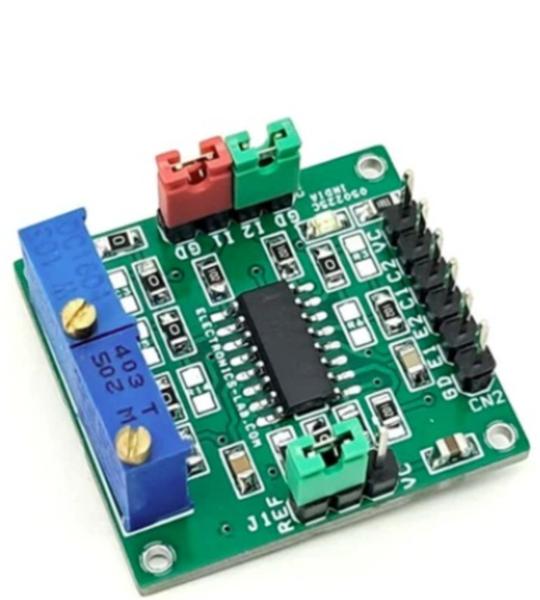
Module is a dual 12-bit PWM-to-voltage output DAC with high accuracy. The board is based on the LTC2644 chip. The LTC2644 measures the period and pulse width of the PWM input signals and updates the voltage output DACs after each corresponding PWM input rising edge. The DAC outputs update and settle to 12-bit accuracy within 8μs typically and are capable of sourcing and sinking up to 5mA (3V) or 10mA (5V), eliminating voltage ripple and replacing slow analog filters and buffer amplifiers. The circuit has a full-scale output of 2.5V using the 10ppm/°C internal reference. It can operate with an external reference, which sets the full-scale output equal to the external reference voltage. Each DAC enters a pin-selectable idle state when the PWM input is held unchanged for more than 60ms. The project operates from a single 2.7V to 5.5V supply and supports PWM input voltages from 1.71V to 5.5V. The PWM frequency can be any frequency between 30Hz and 6. 25kHz. The input level can be between 1.71V and 5.5V, set by a separate IOVCC pin. This project solves many problems associated with filtering a PWM signal to produce an analog voltage, producing a fast-settling, accurate analog voltage in response to a digital PWM input.
Module is a dual 12-bit PWM-to-voltage output DAC with high accuracy. The board is based on the LTC2644 chip. The LTC2644 measures the period and pulse width of the PWM input signals and updates the voltage output DACs after each corresponding PWM input rising edge. The DAC outputs update and settle to 12-bit accuracy within 8μs typically and are capable of sourcing and sinking up to 5mA (3V) or 10mA (5V), eliminating voltage ripple and replacing slow analog filters and buffer amplifiers. The circuit has a full-scale output of 2.5V using the 10ppm/°C internal reference. It can operate with an external reference, which sets the full-scale output equal to the external reference voltage. Each DAC enters a pin-selectable idle state when the PWM input is held unchanged for more than 60ms. The project operates from a single 2.7V to 5.5V supply and supports PWM input voltages from 1.71V to 5.5V. The PWM frequency can be any frequency between 30Hz and 6. 25kHz. The input level can be between 1.71V and 5.5V, set by a separate IOVCC pin. This project solves many problems associated with filtering a PWM signal to produce an analog voltage, producing a fast-settling, accurate analog voltage in response to a digital PWM input.
For standalone operation. Connect a 2.7V to 5.5V supply to the VCC and a GND of CN1 Pin 1 and Pin 4. Connect the IOVCC(IOV) to VCC using Jumper J2 such that the input logic level matches the VCC supply. If a different logic level is required, remove the IOVCC(IOV) jumper and connect the middle pin2 of J2 to a supply equal to the PWM signals’ logic level to the IOVCC(IOV) and GND. There is no sequencing requirement between VCC and IOVCC. Any convenient PWM source can be used to convert the PWM signal into a voltage output.
REF: Reference Output/Input. When the REFSEL jumper is set to INT, the LTC2645’s internal reference can be measured at this point. Nominal impedance is 500Ω. If it is used to drive external circuits it must be buffered appropriately. When REFSEL is set to EXT using Jumper J3, an external reference between 1V and VCC may be connected to this point
LTC2644-L12: Supports Frequency up to 6.25Khz, for higher frequency select below chips.
This is a two Channel high-side switch designed for automotive applications. It has a built-in overcurrent limit function, thermal shutdown protection function, open load detection function, low power output-OFF function etc. It also has a current sensing function of output load current.
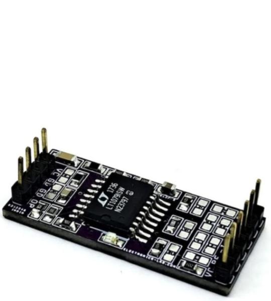
The LT1079 draws very little supply current while still delivering low offset voltage and low noise. This makes the module well-suited to battery-powered instrumentation and sensor front-ends where both precision and low power draw matter.
This is a versatile PWM generator module built around the TL494 PWM control chip. The flexible design allows for multiple component configurations to support various applications. Users can customize the module by installing only the components required for their specific application while leaving out unnecessary components.
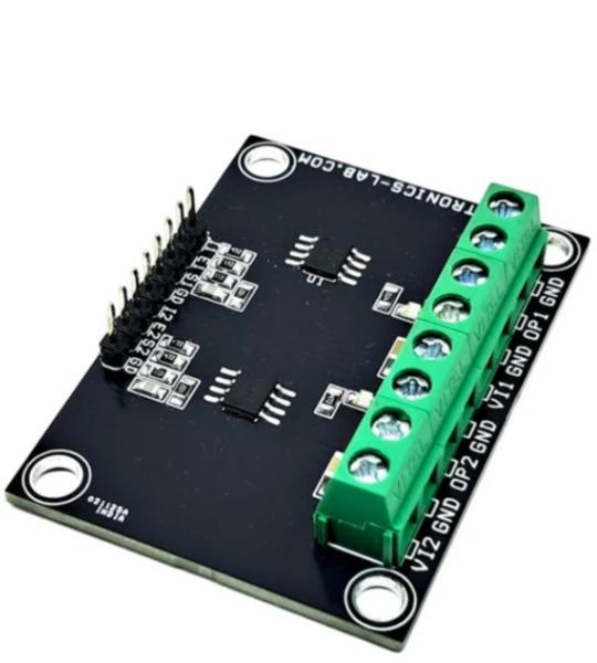
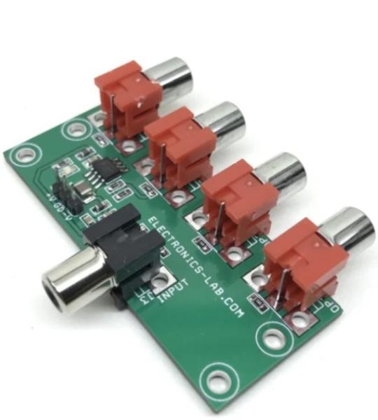
This is a low-cost video distribution amplifier capable of driving up to four video lines. The amplifier is configured with a non-inverting gain of 2. The input video source is terminated in 75 Ohms and is applied to the high impedance non-inverting input. Each output line is connected to the op-amp’s output via 75 Ohms series back termination resistor for proper cable termination. The termination resistor at the other end of the lines divides the output signal by 2, which is compensated by the gain of 2 of the op-amp. The project is built using AD8010 op-amp which is optimized for this specific function of providing excellent video performance in driving multiple video loads in parallel. Significant power is saved and heat sinking is greatly simplified because of the ability of the AD8010 to obtain this performance when running on ±5 V supply. Circuit provides 46dB of output-to-output isolation at 5Mhz driving back terminated 75 Ohms cable. Ferrite beads and high-value ceramic capacitors are used on the power supply input to reduce the noise.
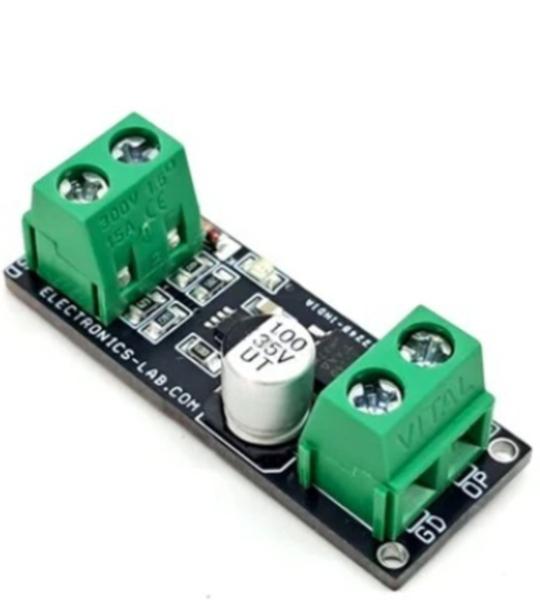
This is a High Voltage Undervoltage (UV), Overvoltage (OV) and Reverse Supply Protection Controller consists of LTC4365 chip and MOSFET. The controller protects the load circuit from input voltages that may be too high, too low or negative. It operates by controlling the gates of two back-back connected MOSFETs to keep the output in safe range. The OV and UV protection levels are adjusted by resistive dividers at the OV and UV pins. Asserting the SHDN pin disables the MOSFETs and places the LTC4365 in a low-current shutdown state. The FAULT pin is asserted when the controller is in shutdown mode or when the input voltage is outside of the UV or OV level. The LTC4365 can withstand DC voltages between -40V and 60V and has a valid operating range 2.4V to 35V. In this project the circuit is optimized for 12V DC, Undervoltage is set to 5V DC and Overvoltage is 18V DC.
Cookie preferences