USD
 INR

Call Us Now
+91 9106756572
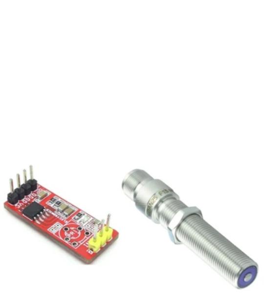
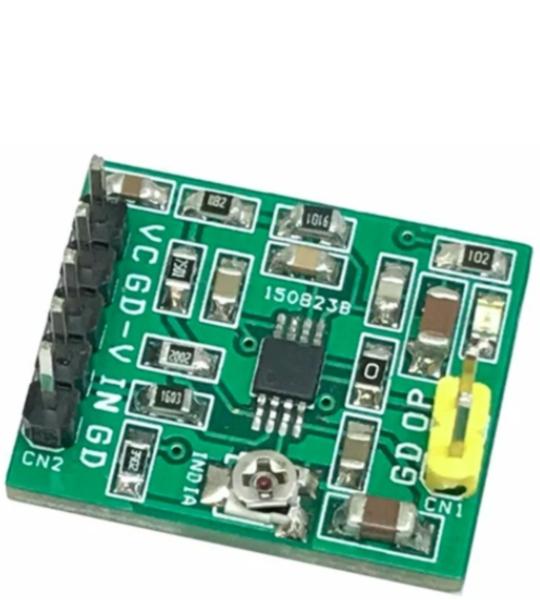
The circuit shown here is a frequency-to-voltage converter that can be used in many applications. This is a signal conditioner for Variable Reluctance Magnetic Pickup Sensor used in engines or machines to detect the speed by sensing gears’ teeth. The input signal level is 20mV to 28V. The circuit provides 1V (67Hz/Volt) when the input frequency is 67Hz with a 15V power supply. The maximum input frequency is 1Khz. The project was built using LM2907N-8 IC, refer to the datasheet of the chip for more information and various configurations. CN1 connector is provided to connect the sensor or input signal. D1 power LED, CN2 Power input, and Voltage output. Use the formula below to calculate voltage output from the desired frequency input.
The project shown here converts bipolar +/-10V (Dual 10V) signal and provides a single-ended 0 to 5V signal. The circuit attenuates a +/-10V, 10Khz bandwidth bipolar signal converts to a single-ended signal, and also filters it by a 3rd-order Butterworth filter to drive a single-ended analog-to-digital converter (ADC). The project was built using OPA2206 OPAMP which protects the input signal from overvoltage up to 40V beyond either supply. The board can be used for applications such as programable logic controllers (PLCs), low-power data acquisition systems (DAQs), and field instruments where high precision, low power, and signal fault protection are needed. OPA2206 is ideal for this application because of the high supply range, high DC precision (4-uV offset and 0.08-uV/C offset drift), and low power consumption (220uA quiescent current) that minimizes the thermal dissipation requirements. Because of the internal OVP topology, the device provides better DC and AC accuracy under normal operating conditions compared to passive external protection and results in a smaller system solution.
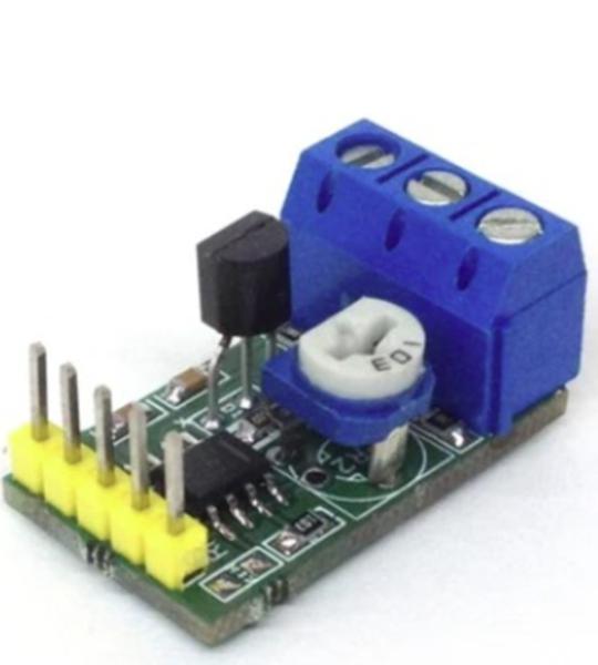
This is an analog input module that helps to digitalize temperature, current (4-20mA) and voltage (±10V) for PLC and Microcontrollers input. This analog module can be used for Programmable Logic Control (PLC), Programmable Automation Control (PAC) and Discrete Control System (DCS). The module has three input terminals. This PLC input accepts inputs of ±10 V or ±20 mA. The output is a single-ended voltage of 2.5 V ±2.3 V (or 200 mV to 4.8 V). Many PLCs typically have this input and output ranges. PR1 Trimmer potentiometer provided to fine trim the gain. Ideally, PR1 + R1 value should be 10.5Khoms. The circuit works with dual supply +/-15V DC. The circuit is from Texas instruments INA828 datasheet.
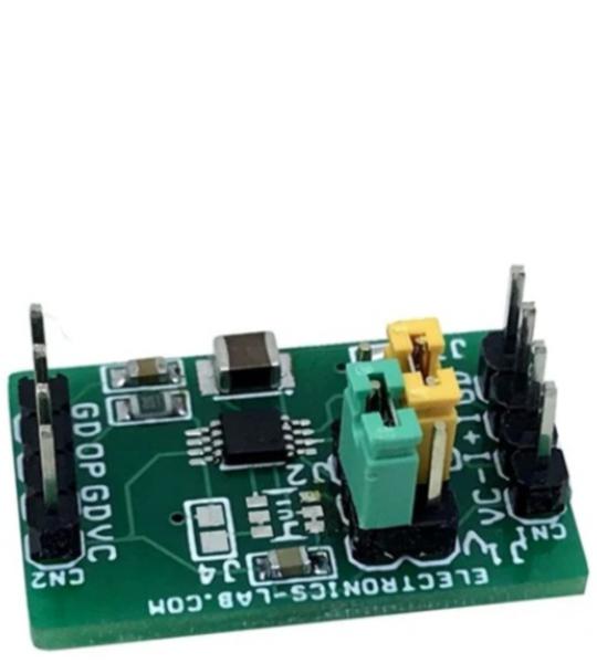
The circuit shown here is a high-side voltage-to-current (V-I) converter. It translates an input voltage of 0 V to 2 V to an output current of 0 mA to 100 mA. The low offset voltage and offset drift of the OPA2333 facilitate excellent DC accuracy for the circuit.
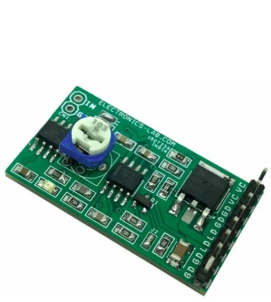
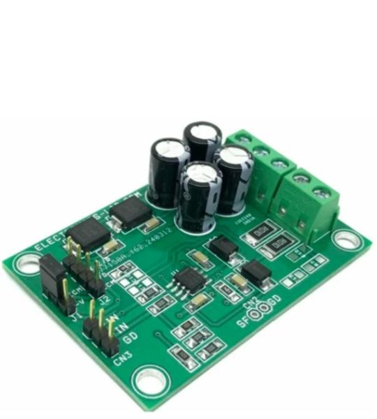
The project provides a high-side current source that supplies an adjustable current to a ground reference load. The first op-amp stage sets a reference current based on the input control voltage. The second op-amp stage acts as a current mirror that gains the reference current and regulates the current sourced from the output PMOSFET Q2 to the load. R2, R4, and R10 set the output current based on the input control voltage. Components C7, R9, R8, R7, C6, R3 provide compensation to ensure stability of the circuit.
This board will make your work easy if you want to interface +/- 10V (Dual 10V) device or sensor to single-supply signal ADC. This tiny project has been made for industrial and process control applications and provides an easy interface between +/-10V (Dual 10V) sensor or device to single-supply ADC. Connect +/-10V sensor/device to pin 3 of connector CN1, and circuit outputs 0.5V to 4.5V at pin 3 of connector CN2. The operating supply of the circuit is 5V and it draws few milliamps of current. The project is also provided with optional precision Ref voltage for accurate output.
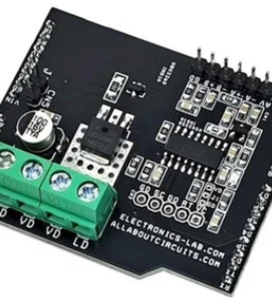
The Kilo Lamp is an interactive lamp controller built using an Arduino Uno shield. It also contains a load cell, a load cell amplifier, and a MOSFET that drives an LED using a pulse-width modulated (PWM) signal. The brightness of the LED is determined by how much weight is placed on the lamp. When the load reaches 5 kg, the lamp achieves 100% brightness
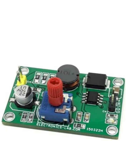
This is a high-efficiency and reliability DC/DC converter with a dimming feature for super high brightness LEDs. The project is built using L6902D chip. L6902 is a complete and simple step-down switching regulator with adjustable current limit. The current control loop with external sense resistors R6, R7, and R8 are able to work in constant current mode providing up to 350mA output current with an accuracy of 5%. Potentiometer PR1 helps to control the dimming of the LEDs. PR1 is connected to the 3.3V reference pin of the chip. When the dimming (CS+) pin is grounded (0V) the maximum output current is provided (350mA) and vice versa when 3.3V is applied to the pin, the current provided is zero and so the LED is off.
This is a mini flasher board that can drive high-power LED or a lamp, mainly designed for automotive applications. The project consists BD9555FVM-C timer chip and MOSFET. The circuit is configured as a flasher, and can also be used as a PWM driver with an adjustable duty cycle and frequency. Capacitors C2, R4, and PR1 can be used to set the duty cycle. Please refer to the datasheet of BD9555FVM for more information. N-channel IRF7862 MOSFET used to drive the load, and it’s advisable to use maximum load current 3A due to small thermal dissipation on PCB for the MOSFET. The operating power supply is 5V to 15VDC.
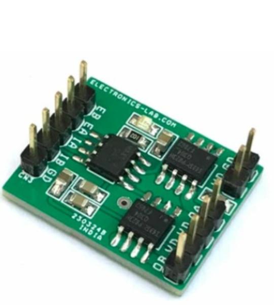
This is a low profile and small size two-channel MOSFET board that can drive loads up to 2 x 3A. The Power Supply is 5V to 14V DC. Inputs and input Enable are TTL-level signals. The Output is by default enabled and an active high signal disables the output. Parallel Operation of Dual Outputs for Larger Driver Output Current is possible. The Circuit can drive a high-speed PWM signal as well as ON/OFF signal.
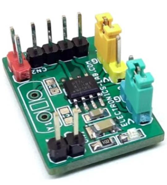
This is an easy-to-build project and it is the most cost-effective and high-performance frequency multiplier, which instigates analog phase lock loop techniques. The circuit provides high-quality, high-frequency output from lower frequency crystal or clock input. The project can be used as a crystal frequency oscillator, clock multiplier and frequency translation. Using phase-locked-loop (PLL) techniques, the device uses a standard fundamental mode, inexpensive crystal to produce an output clock up to 200Mhz. On-board jumpers are provided to select from nine different multiplication factors, which output many common frequencies. The device also has an output enable pin that tri-states the clock output when the enable pin is taken low. The chip is intended for clock generation and frequency translation with low output jitter.
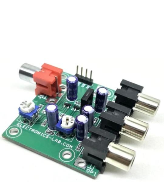
If you need to drive multiple video gadgets or monitors from a single video signal source then this board is the right choice for you. This is a 3-channel video splitter with an amplifier and the circuit is built using discrete components. Q2 and Q1 act as a signal amplifier, Q3 act as output driver, trimmer potentiometer PR1 is provided to adjust the input signal swing, PR2 Trimmer is provided to set the gain of the amplifier, D1 is the power LED. The operating power supply is 12V DC and it draws 100mA current. RCA Connector J4 is the Video signal input, RCA Connector J1, J2, J3 provide the outputs. The default gain of the circuit is 4. The bandwidth is 5Mhz, input and outputs impendence are 75 Ohms. It is important to use all 3 channels at a time or change R11 to 150 Ohms if you will only use 1 x channel or 82 Ohms if 2 x channels are in use. Adjusting the board is very easy, just connect a voltmeter at the base of Q2 and adjust the PR1 so the voltage at the base of Q2 is 1V.
This module provides a platform to evaluate the OPA462 high-voltage, high-current operational amplifier. Multiple component footprints allow the most common circuit configurations. The board accommodates high-voltage and high-current operational amplifier OPA462 from Texas Instruments. A High-Voltage Noninverting Amplifier, AV = 17 V/V. An example application circuit is given below. The board is capable of operating with supply voltages as high as ±90 V (180 V), or as low as ±6 V (12 V). The high-voltage process and design of the OPA462 allow the device to be used in applications where most operational amplifiers cannot be applied, such as high-voltage power-supply conditions, or when there is a need for a very high-output voltage swing. The output is capable of delivering up to ±30 mA output current or swinging within a few volts of the supply rails at moderate current levels. The OPA462 features input overvoltage protection, output current limiting, thermal protection, a status flag, and enable-disable capability. The output swing is 85V with 5V AC signal input and frequency 10Khz. Status Flag is an open-drain active-low output referenced to E/D Com. This pin goes active for either an overcurrent or overtemperature condition. Close (Link) Shunt between GD and E/D Com to enable the output, and Close E/D and E/D Com Jumper J2 to disable the Output.
Cookie preferences