USD
 INR

Call Us Now
+91 9106756572
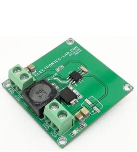
This powerful buck converter can efficiently produce 5 V@4A with an input voltage between 7V to 31V. The project is built using the NR110E chip from Sanken Semiconductor. The IC integrates the power MOSFET. With current mode control, ultra-low ESR capacitors, such as ceramic capacitors are used. The ICs have protection functions such as Overcurrent Protection (OCP), Undervoltage Lockout (UVLO), and Thermal Shutdown (TSD). An adjustable Soft-start by an external capacitor C4 prevents the excessive inrush current at start-up. The feature of increasing efficiency at light loads allows the project to be used in energy-saving applications. Due to the ICs integrating phase compensation circuit the number of external components count is low. Screw terminal provided for easy input and output connections. D2 Power LED indicates the output. The project provides an efficiency of up to 94%.
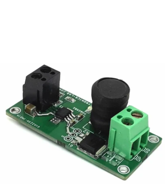
The step-down DC-DC Converter project presented here provides 3.3V @ 1A output from an input range of 8V to 36V DC. The adjustable current limit is an important feature of the project, which prevents the device from accidental output short circuits avoiding excessive load damage. The internal limiting current (latched function) has a typical value of 2.5 A. The project is built around the L6902 chip from ST. The L6902D is a complete and simple step-down switching regulator with an adjustable current limit. Based on a voltage mode structure it integrates a current error amplifier to have a constant voltage and constant current control. By means of an onboard current sense resistor R1 and R2, current limit programming is very simple and accurate (±5%). Refer to the datasheet of the chip for R1 and R2 values about the current limit adjustment. The project can be used to charge NiMH and NiCad batteries due to its constant current feature. The project operates with a fixed switching frequency of 250Khz. If the temperature of the chip goes higher than a fixed internal threshold (150°C with 20°C hysteresis), the power stage is turned off. Other protections besides thermal shutdown complete the device for a safe and reliable application: overvoltage protection, frequency foldback overcurrent protection, and protection vs. feedback disconnection.
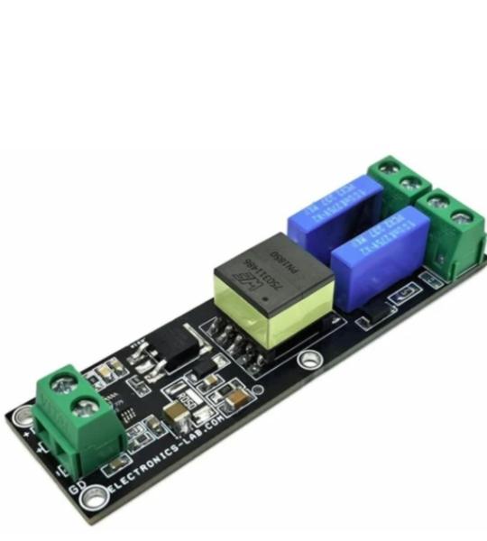
This is an isolated flyback converter featuring the LT3748 chip from Analog Devices. The circuit is designed for a +/-340V DC (2 x 340V) output from a 7V to 15VDC input. The output current is up to 2 x 8mA. The board senses the isolated output voltage directly from the primary side flyback waveform during the off time of the power switch. No third winding, optocoupler, or signal transformers are required for regulation. A minimum load of approximately 2% of the maximum load is required on the output to maintain regulation.
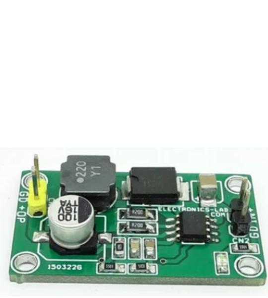
This is a synchronous step-down DC/DC converter based on the RT7258 chip. The chip has integrated high-side internal power MOSFET and gate driver for a low-side external power MOSFET. The board delivers 3.3V DC – 5A output current from 10V to 24V input supply. The RT7258‘s current mode architecture allows the transient response to be optimized over a wide input voltage and load range. Cycle-by-cycle current limit provides protection against shorted outputs and softy-start eliminates input current surge during start-up.
This is a Phase-Shifted Full-Bridge PWM LM5046 carrier board that contains all of the features necessary to implement a phase-shifted full-bridge topology power converter. All inputs and outputs pins are accessible using the header connector. High efficiency DC-DC converter can be created using LM5046 carrier board + External H-Bridge and Transformer. Refer to the datasheet of LM5046 and schematic to configure the frequency, current feedback, delays, etc.
The circuit shown here is a low-cost electronic DC load designed to sink current from a power source. This test equipment can be used to test power devices such as power supplies, chargers, solar panels, and batteries. The board is built using op-amp TLE2141, LM385 provides the reference voltage. Resistor R11 acts as a shunt resistor and provides load current feedback to the op-amp, potentiometer P1 is provided to adjust the load current, and D1 is the power LED. A 10-turn Potentiometer is provided for fine current adjustment. The user may use a single-turn PR1 trimmer potentiometer. The load current range is up to 2.5A, and the project can handle higher currents with large-size heat-sink and forced air using a Fan. You may use a 0 to 5A Current Meter in series to measure the load current.
Project provides 1.2 to 20V DC output with current limiter adjustable to 0-5A. I have tested the circuit with 250mA output without a heat sink. Project is capable to drive 3A continues load and 5A peak, large size heat sink required for full load. The tiny power supply based on low cost OPA548 high-voltage and high-current operational amplifier is ideal for driving a wide variety of loads. The project provides excellent low-level signal accuracy and high-output voltage and current. The circuits operate with single supply 24V DC and logic supply 5V DC. The IC is internally protected against over-temperature condition and current overload. Trimmer potentiometer PR1 sets the output voltages, PR2 helps to set the current limit 0 to 5Amps.
This is a tiny module that allows users to charge small Li-ion batteries, CR2032 or equivalent, from a low power source such as a small photovoltaic cell. The project consists of the LTC3105 step-up DC-DC converter chip which features Maximum Power Point Control (MPPC) and 250mV start-up voltage which enables operational directly from low power, high impedance alternative power sources such as photovoltaic cells. A user-programmable MPPC set point maximizes the energy that can be extracted from any power source. Burst Mode operation, with a proprietary self-adjusting peak current, optimizes converter efficiency and output voltage ripple overall operating conditions. The circuit works with single-cell or dual-cell in parallel. The operating supply of this project is as low as 225mV and a maximum of 5V. Input supply should not exceed 5V DC. The module is programmed to output 4.1V which is important to charge the Li-On battery. Jumper J1 should be open for normal operation, close to disable the output.
This over-current latch load switch provides over-current protection, thermal shutdown protection, soft-start function, and low power OFF function. The Overcurrent protection function is activated when the load is shorted. This protection function is effective in preventing damage due to sudden and unexpected incidents. It is also equipped with an error flag notification pin which indicates thermal shutdown and over-current condition. The project can help to protect the connected device from overcurrent, monitoring of various power lines, and power management. The board operates from 12V DC to 24V DC. The power LED indicates the output. Screw terminals provided for an easy connection of input and output supply. For the Fault function, additional 5V VCC DC input is required, otherwise, the VCC is not required. The circuit is normally enabled, and you can connect enable pin to GND to disable the output. Output is latching type; power is OFF when a fault condition occurs and sequence can be reversed with power OFF or Disable/Enable Pin.
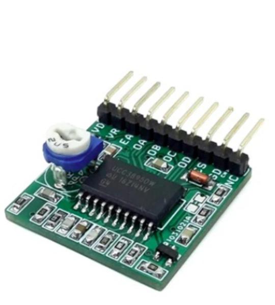
This is a Phase-Shifted Full-Bridge PWM UCC3895 carrier board that contains all of the features necessary to implement a phase-shifted full-bridge topology power converter. All inputs and outputs pins are accessible using a header connector. A highly-efficient DC-DC converter can be created using this carrier board + External H-Bridge and Transformer. Refer to the datasheet of UC3895 and schematic to configure the working frequency, current feedback, delays, etc.
3A TEC Driver Module is a complete power stage solution to drive Thermoelectric Cooler (TEC). The required DC voltage input controls the output current. It consists of the Texas instruments DRV593 power driver IC, along with a few discrete passive components required for operation. It also includes jumpers for configuring the features of the device, LEDs for fault monitoring, and an output filter. The 4 Pin header connector for the inputs, 4-pin header connector for output, and 4 Pin header connector for the power supply provide ease of connection to any system, from an existing design to a bread-boarded prototype. Connect a dc control voltage to CN1 Pin 3 (IN+), ranging from ground to VCC. The Pin 7 of the IC is held to VCC/2 with a resistor voltage divider, as shown in the schematic. Therefore, a dc control voltage of VCC/2 provides 0-V output from PWM to H/C. Input DC voltage range is 1.2V to 3.8V when the supply voltage is 5V and 1.2V to 2.1V when the supply voltage is 3.3V.
This is a low-cost boost converter that converts a 3.3V input to 5V at 250mA load current. The LM2578A chip is used to build this project. The LM2578A is a switching regulator which can easily be set up for such DC-to-DC voltage conversion circuits as the buck, boost and inverting configurations. In this board, the IC is configured as a boost converter. The operating frequency is 50Khz.
Cookie preferences